Layers
Eagle separates the parts of your design into layers. Each layer corresponds to a different characteristic of your final design.
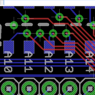
The most important layers are Top and Bottom. These are your copper layers, and define how the copper on your PCB will be etched.
The layers you'll need to know about are:
Top- The top copper layer (red)Bottom- The bottom copper layer (blue)Dimension- The outer dimensions or shape of your PCB (light gray)tPlace- Silkscreen placed on the top (dark gray)bPlace- Silkscreen placed on the bottom (dark gray)
There are other layers, but Eagle uses most of them automatically. For example; vias will always live on the vias layer and pads on the pads layer.
Showing & Hiding Layers
Your design can become busy and confusing. You should hide layers you're not working on. tPlace and bPlace are common choices.
You can hide a layer with the display command, or dis for short. dis accepts by a list of layers you want to show or hide. Prefix a layer name with a minus - to hide it.
dis -tPlace
Or hide more than one by typing:
dis -tPlace -bPlace
You can hide all layers except the ones you want to work on by typing:
dis none top bot via pad
And show everything by typing:
dis all